AED 8.00
Description
The LM324 is a four-amplifier operational amplifier (Op-amp). The device is inexpensive and has real differential inputs. The LM-324 can function at low voltage levels of up to 3V and at high voltage levels of up to 32V. no requirement for outside bias. This product complies with RoHS regulations and is lead (Pb) and halogen-free. Conventional amplifier circuits, transducer amplifiers, DC gain blocks, etc. are some examples of LM324 real-world applications.
Package Includes:
- 1 x Operational Amplifier LM324N DIP
Features:
- 4 independent amplifiers.
- Some of the variants are short-circuit protected at the output.
- True differential input stages.
- Frequency compensated within IC for unity gain
- DC voltage gain is large that is 100 dB
- Bandwidth is Wide that is 1 MHz
- The range of power supply is wide, and for single voltage supply ranges from 3volts to 32volts
- Basically independent for supply voltage
- The range of differential i/p voltage is equivalent to the voltage power supply.
- O/p voltage swing ranges from 0V to V+ & − 1.5V
Description:
An operational amplifier (Op-amp) with four channels is the LM324. The device is inexpensive and has real differential inputs. The LM 324 is a better operational amplifier than the others for applications requiring a single supply. The LM-324 can function at low voltages of up to 3V and at high voltage levels of up to 32V. The common mode input range of the LM-324 covers negative supply, which avoids the requirement for external biasing and is one of its main advantages. The output voltage range also includes the negative power supply voltage. This gadget complies with RoHS regulations and is lead (Pb) and halogen-free. Each package contains four amplifiers. Conventional amplifier circuits, transducer amplifiers, DC gain blocks, and other real-world applications for the LM 324 are available.
Principle of Work:
Op amps are essentially multistage amplifiers with extremely intricate connections between their various amplifier stages. Numerous transistors, FETs, and resistors make up its internal circuit. All of this takes up very little room. Therefore, it is available in the form of an Integrated Circuit (IC) and is packaged in a compact box. An amplifier that can be set up to carry out different operations, such as amplification, subtraction, differentiation, addition, and integration, is referred to as an "op amp." Two input terminals and one output terminal compensate for an op-amp. There are two voltage supply terminals on the op-amp as well. The differential input is made up of two input terminals. We refer to the terminal of the operational amplifier denoted by a negative (-) sign as the inverting terminal and the terminal denoted by a positive (+) sign as the non-inverting terminal. The amplified output signal is 180 degrees out of phase with respect to the applied input signal if an input signal is supplied to the inverting terminal (-). The output signal will be in phase, or without phase shift with respect to the input signal, if we apply an input signal to the non-inverting terminal (+).

A single power source can run an LM324 device. It's also possible to use two power sources. Pins 4 and 11 are the terminals or pins that are utilized. The four OP-AMPs can be powered by either one or two of these supplies. The first OP-inverting AMPs and non-inverting inputs are applied at pins 2 and 3, respectively. At pin number 1, the first OP-output AMPs can be found. Inverting input is applied to pin number 6 for the second OP-AMP and non-inverting input to pin number 5. At pin number 7, the second OP-output AMP is acquired. Inverting input is applied to pin 9 of the third OP-AMP, whereas non-inverting input is applied to pin 10. At pin number 8, the third OP-output AMP can be found. Inverting input is applied to pin 13 of the fourth OP-AMP whereas non-inverting input is applied to pin 12. At pin number 14, the fourth OP-output AMP's can be found.
Pinout of the Module:
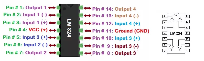
| PINS | Description |
|---|---|
| 1 (Out 1-Output 1) | This pin is for obtaining the output of 1st OP-AMP |
| 2 ( Input 1-inverting Input) | This pin is for applying an inverting input voltage to 1st OP-AMP |
| 3 ( Input 1- non-Inverting Input) | This pin is for applying non-inverting input voltage to 1st OP-AMP |
| 4 (Vcc) | This pin is for connecting supply voltage. |
| 5 ( Input 2- non-Inverting Input) | This pin is for applying a non-inverting input voltage to 2nd OP-AMP |
| 6 ( Input 2-inverting Input) | This pin is for applying an inverting input voltage to the 2nd OP-AMP |
| 7 (Out 2- Output 2) | This pin is for obtaining the output of the 2nd OP-AMP |
| 8 (Out 3- Output 3) | This pin is for obtaining the output of the 3rd OP-AMP |
| 9 ( Input 3-inverting Input) | This pin is for applying an inverting input voltage to the 3rd OP-AMP |
| 10 ( Input 3- non-Inverting Input) | This pin is for applying non-inverting input voltage to the 3rd OP-AMP |
| 11 (Vee, GND) | This pin is for connecting ground for single voltage operation or the second as Vee for dual power supply operation |
| 12 ( Input 4- non-Inverting Input) | This pin is for applying non-inverting input voltage to the 4th OP-AMP |
| 13 ( Input 4-inverting Input) | This pin is for applying an inverting input voltage to the 4th OP-AMP |
| 14 (Out 4- Output 4) | This pin is for obtaining an output of 4th OP-AMP |
Applications:
- Audio mixers.
- AC inverters.
- VF drives.
- Oscilloscopes.
- Systems with DLP front projection.
- Solar inverters.
- Uninterruptible Power Supply (UPS).
- A quadruple oscillator,
Circuit:
LM324 IC-based Cell phone Detector Circuit Diagram
This circuit's design is fairly straightforward, and it may be used to find a cell phone at a distance of between 10 and 20 meters. Due to the individual signal production capabilities of each mobile device, the detection range can largely rely on the device. The voice contents are not detected by this circuit; only the encoded signal is. The cell phone can make calls while sending and receiving SMS messages, or it can receive the encoded signals when it gets a call. This circuit has multiple uses, including detecting a missing phone and locating a cell phone in restricted places.
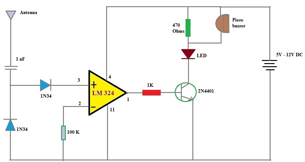
The circuit's beating heart is the LM324 operational amplifier. Four high gain operational amplifiers are present in this IC. However, this circuit only makes use of one of the four op-amps. To turn on the LED and the piezo buzzer, a transistor 2N4401 is connected to the LM324's output. Additionally, the number of LED connections can be increased to 25. The circuit can be run between 4.5 and 12 volts DC. We must change the value of a current limiting resistor for each LED in the circuit from 470 ohms to 220 ohms if the circuit is used below 9V (lower voltage). A variable resistor with the value of 100K can be used to alter the sensitivity of the circuit.
Library:
No Library is needed for this IC to function
Code:
No code is needed for this IC to function
Technical Details:
| Parameters | LM324 |
|---|---|
| Input offset voltage (mV) | 3 |
| Input bias current (nA) | 100 |
| Input Offset Current (nA) | 30 |
| Input Common Mode Voltage Range (V) | -1.5 |
| Large signal voltage gain (V/mV) | 100 |
| Supply current (mA) | 3.0 |
| Common mode rejection ratio (dB) | 85 |
| Amplifier-to-Amplifier Coupling (dB) | -120 |
| Supply voltage Rejection Ratio (dB) | 100 |
| Supply Voltage (V) | 32 |
| Power dissipation-PDIP (mW) | 1130 |
| Power dissipation-CDIP (mW) | 1260 |
| Power dissipation-SOIC Package (mW) | 800 |
| Junction-to-ambient thermal Resistance (°C/W) | 88 |
| Differential Input voltage (V) | 32 |
| Output Short Circuit to Ground (Single Amplifier) | Continuous |
| Lead temperature (Soldering, 10s) (°C) | 260 |
| Junction temperature (°C) | 70 |
Resources:
Comparisons:
The LM324 comes in a DIP-14 package, which is smaller than the DIP-14 package that the LM358 comes in, and this is the only significant variation in the specification. The LM324 can dissipate more power than the LM358 because of this. This could possibly be the reason why the LM324's offset voltage drift has increased.
|
Specification |
LM358 |
LM324 |
|
Supply voltage |
32V |
32V |
|
Power dissipation |
830mW (DIP) |
1130mW (DIP) |
|
Input offset voltage |
5mV |
5mV |
|
Input offset voltage drift |
20µV/C (max.) |
30µV/C (max.) |