AED 5.25
Description
The 74HC266N is a quad XNOR (exclusive-NOR) gate integrated circuit that consists of four individual logic gates in a single package. Each gate has two inputs and one output that produces a high output only when both inputs are the same (both 0 or both 1), otherwise, the output is low. The 74HC266N operates on a 2-6V supply voltage range and is compatible with standard TTL and CMOS logic families. It is commonly used in digital logic applications such as signal processing, control systems, and computer memory.
Package Includes:
- 1 x Logic Gate XNOR 74HC266N
Features:
- Quad XNOR gate: The IC consists of four individual XNOR gates in a single package, providing a convenient and space-saving solution for logic operations.
- Input/output voltage range: The IC operates on a supply voltage range of 2-6 volts, making it compatible with standard TTL and CMOS logic families.
- High-speed performance: The IC provides fast switching speeds and low propagation delay times, allowing it to perform logic operations quickly and efficiently.
- Low power consumption: The IC has low power consumption, making it suitable for battery-powered applications and other low-power devices.
- Wide operating temperature range: The IC can operate within a wide temperature range of -40°C to +125°C, making it suitable for use in a variety of environments.
- Small form factor: The IC is available in a compact 14-pin DIP, making it easy to integrate into electronic designs.
Description:
The 74HC266N is a member of the 74HC family of high-speed CMOS logic devices, which are designed for use in a variety of digital logic applications. It is a quad (four-input) XNOR (exclusive-NOR) gate, which means that each gate has two input pins and one output pin. The gate produces a high output signal only when both inputs are the same (both 0 or both 1), and a low output signal when the inputs are different (one 0 and one 1). The XNOR gate is a logical complement of the XOR (exclusive-OR) gate, which produces a high output signal when the inputs are different and a low output signal when they are the same. The XNOR gate is used in a variety of digital logic applications, such as signal processing, control systems, and computer memory. The 74HC266N operates on a supply voltage range of 2-6 volts and is compatible with standard TTL and CMOS logic families. It has a maximum input current of 1 microampere and a maximum output current of 5.2 milliamperes. The device is available in a 14-pin DIP (dual in-line package). The 74HC266N provides fast switching speeds and low power consumption, making it an ideal choice for high-performance digital logic applications. Its small size and low cost also make it a popular choice for use in integrated circuits and other electronic devices.
Principle of Work:
The 74HC266N XNOR gate IC works on the principle of exclusive-NOR logic. It consists of four individual XNOR gates, each with two input pins (A and B) and one output pin (Y). The logic function of the XNOR gate is to produce a high output signal only when both inputs are the same (both 0 or both 1), and a low output signal when the inputs are different (one 0 and one 1). The IC is designed using CMOS technology, which allows it to operate on a low supply voltage and consumes minimal power. Each XNOR gate in the IC consists of a network of transistors and resistors that implement the exclusive-NOR logic function. When both inputs to an XNOR gate are the same, the output transistor is turned on and produces a high output signal. When the inputs are different, the output transistor is turned off and produces a low output signal. The IC provides fast switching speeds and low propagation delay times, allowing it to perform logic operations quickly and efficiently.
Pinout of the Module:

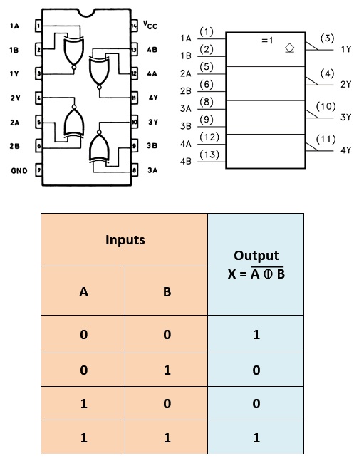
The pinout of the 74HC266N XNOR gate IC is presented in the next table :
| Pin No. | Pin Name | Function |
|---|---|---|
| 1 | A1 | Input A for gate 1 |
| 2 | B1 | Input B for gate 1 |
| 3 | Y1 | Output Y for gate 1 |
| 4 | GND | Ground |
| 5 | A2 | Input A for gate 2 |
| 6 | B2 | Input B for gate 2 |
| 7 | Y2 | Output Y for gate 2 |
| 8 | Vcc | Supply voltage |
| 9 | A3 | Input A for gate 3 |
| 10 | B3 | Input B for gate 3 |
| 11 | Y3 | Output Y for gate 3 |
| 12 | A4 | Input A for gate 4 |
| 13 | B4 | Input B for gate 4 |
| 14 | Y4 | Output Y for gate 4 |
The IC has four individual XNOR gates, each with two input pins (A and B) and one output pin (Y). The inputs are on pins 1, 2, 5, 6, 9, 10, 12, and 13, and the outputs are on pins 3, 7, 11, and 14. Pin 4 is the ground (GND) pin, and pin 8 is the supply voltage (Vcc) pin.
the truth table for the 74HC266N XNOR gate IC:
| Input A | Input B | Output Y |
|---|---|---|
| 0 | 0 | 1 |
| 0 | 1 | 0 |
| 1 | 0 | 0 |
| 1 | 1 | 1 |
As you can see, the output Y is 1 only when both inputs A and B are the same (either 0 and 0 or 1 and 1). When the inputs are different (0 and 1 or 1 and 0), the output Y is 0. This logic function of the XNOR gate is useful in digital circuits for comparing two binary values and determining whether they are equal or not.
Applications:
- Binary Comparators: The XNOR gate can be used to compare two binary values and determine if they are equal. In combination with other logic gates, the IC can be used to implement binary comparators.
- Parity Checkers: The IC can be used to implement parity-checking circuits. Parity checkers are used to detecting errors in digital data transmission and storage systems by adding an extra bit to the data stream that indicates whether the number of bits with a value of 1 is odd or even.
- Arithmetic Circuits: The XNOR gate can be used in arithmetic circuits to perform operations such as addition, subtraction, and multiplication.
- Memory Circuits: The IC can be used in memory circuits to store and retrieve binary data. The XNOR gate can be used as a part of address decoding circuits, which enable the selection of a specific memory location for reading or writing data.
- Control Circuits: The IC can be used in control circuits for various applications, such as motor control, switch debouncing, and power management.
Circuit:
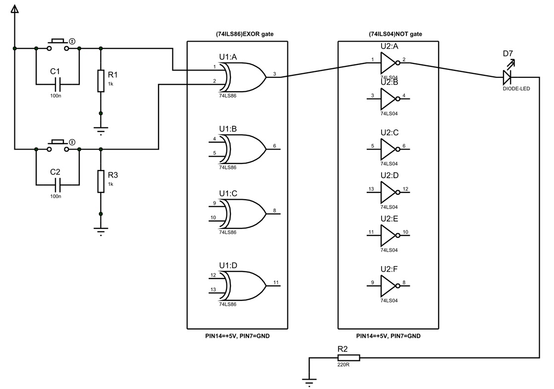
In this circuit utilizing an XNOR gate, we are grounding both inputs of the gate via a 1KΩ resistor. The inputs are then connected to a power source via a button. Pressing the button causes the corresponding pin of the gate to become high. With two buttons, we can effectively simulate the truth table of the EXNOR gate. When one of the buttons is pressed, one input of the gate becomes high while the other input becomes low, resulting in low output.

To counteract the bouncing effect of the button, a capacitor is included in the circuit. If a capacitor is not used, the counter may count events erroneously. It is necessary to include the pull-down resistors in the circuit, as the chosen CHIP is positive edge triggering. Neglecting the resistors may result in unpredictable circuit behavior. While not mandatory, the capacitors are used to neutralize the bouncing effect of the buttons. Including capacitors may improve the performance of the XNOR gate.
Library:
No library Needed
Code:
No Code Used.
Resources:
Comparisons:
The 74HC266 and 74SL266 are both ICs designed to perform the XNOR logic function. However, there are some significant differences between these two ICs:
- Technology: The 74HC266 is a CMOS-based IC, while the 74SL266 is based on Schottky TTL technology. This means that the 74SL266 operates at a faster switching speed than the 74HC266, but it also consumes more power.
- Power Consumption: The 74HC266 is a low-power device, with a typical power dissipation of 4.5mW. In contrast, the 74SL266 is a high power device, with a typical power dissipation of 70mW.
- Voltage Levels: The 74HC266 operates at a wider range of voltage levels, from 2V to 6V, while the 74SL266 operates at a narrower range of voltage levels, from 4.75V to 5.25V.
- Noise Immunity: The 74HC266 has higher noise immunity than the 74SL266, with a typical noise margin of ±1V at a supply voltage of 4.5V. The 74SL266 has a lower noise immunity, with a typical noise margin of ±0.4V at a supply voltage of 5V.